- Details
Instrument Cluster Update 3
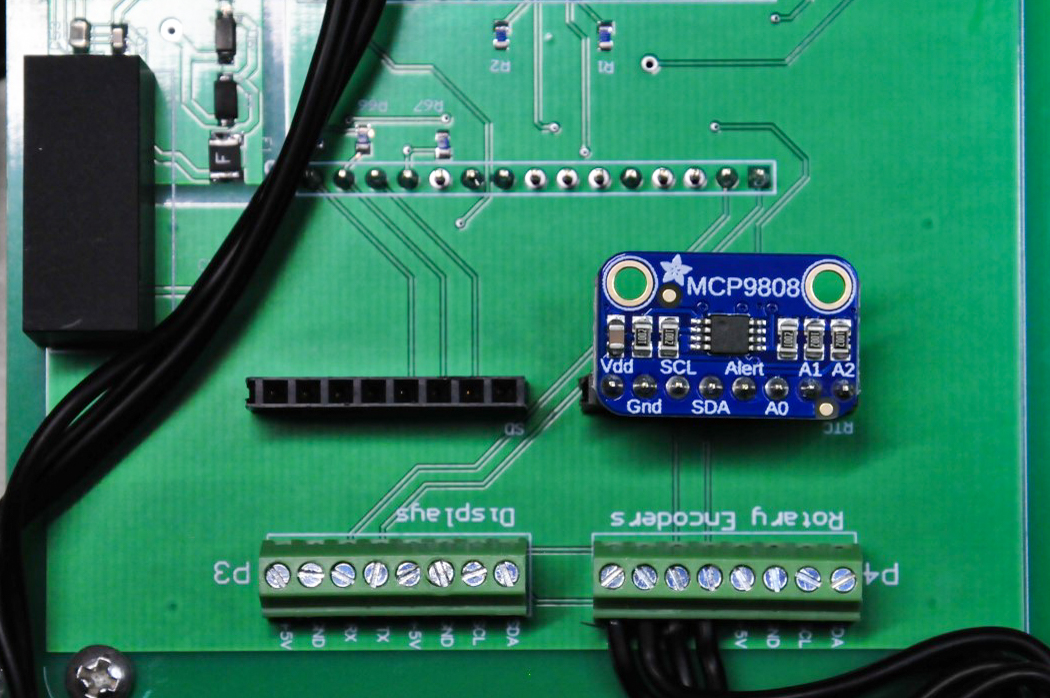
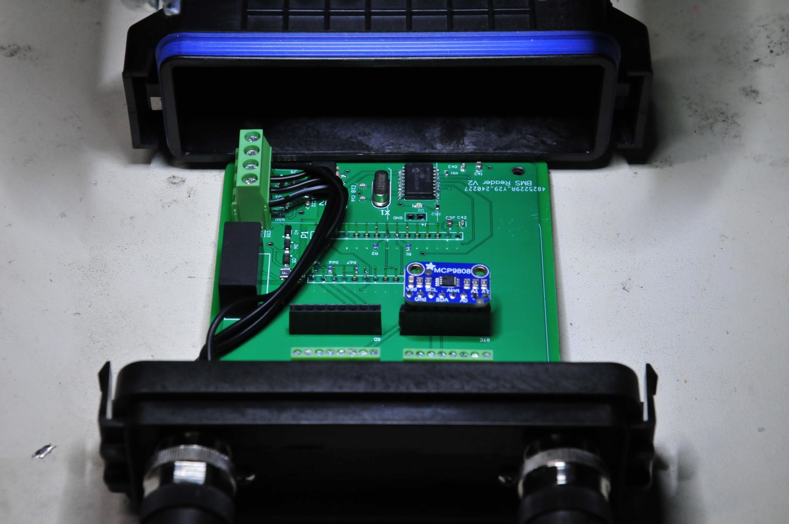
After the crazy hot days we had at the end of June 2025, I was driving my car and wondered what the outside temperature was. Of course I could just look on my phone, but I thought it would be a great update to have the outside and or inside temperature displayed on the 7-segment display in the bottom center of the tachometer. The temperature of the inverter can already be displayed on the 7-segment. I found another great little PCA made by Adafruit, the MCP9808, pictured below. The details can be found here. It is a precision temperature sensor and it communicates the temperature with I2C. Probably way more precise temperature measurement than I need, but it is very inexpensive and easy to use with my designs. I used one of the early versions of the BMS Reader PCAs (blog post) for a temperature reading system to use with the MCP9808. The PCA was already built up with the 12V power isolation, CAN BUS, Arduino Nano Every and screw terminals. Because the Nano Every runs at 5V the I2C communication can be transmitted on wires to several feet without any issue or need for I2C line drivers. Also, it has the same pinout as the Adafruit RTC so the temperature sensor can be plugged into the Reader PCA in the same place (shown in the photo below). The image below is of a Reader PCA that is wired for the CINCH enclosure, the same system I am using with the BMS Reader. I also used the 12mm connectors to connect +12V, CAN BUS and the I2C connection to a sensor mounted in the engine compartment.
The I2C address on the MCP9808 can be set to any of the bottom three bits of the I2C address, so up to eight different addresses are available. More than one MCP9808 can be used or other I2C components on the same I2C connection can be used. The temperature is read by the Reader PCA and then it is formatted and sent on the CAN BUS so the LEVID can read it and display the temperature on the 7-segment.
- Details
Instrument Cluster Update 2
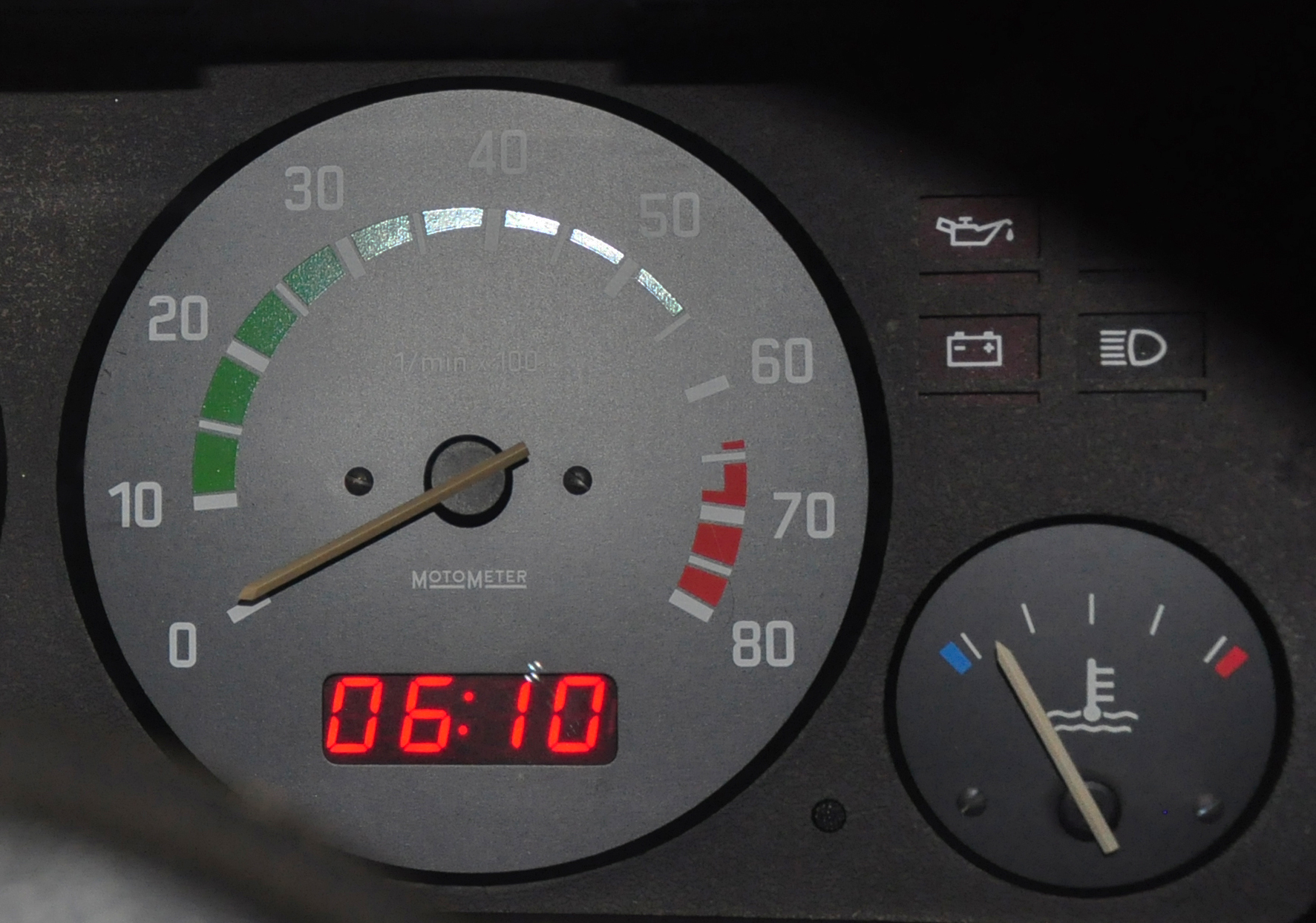
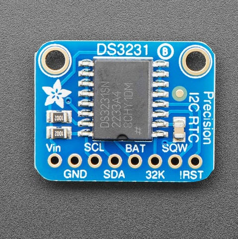
Since the update to the Instrument cluster I made last year (link), it has been working really well except for the Real Time Clock (RTC). The clock is part of the circuit for the 7-Segment LED display that is in the center of the Tachometer, as shown in the image below. The 7-Segment display is used to display all the electric vehicle data, like temperature, voltage, current, and RPM digitally, to complement the analog instruments. It is also used for displaying the time. The RTC is mounted on a daughter board, that is part of the Legacy Electric Vehicle Instrument Driver (LEVID). That PCA controls the startup of the car and controls all the instruments in the instrument cluster. The PCA and the daughter board with the RTC can be seen in the blog post on the instrument cluster update (link). I found that the circuit on the daughter board that was buffering the clock data has failed now for the third time, since the update. The RTC still works, but there is no communication to the processor because of the failed component. The 7-segment display can still show all the electric vehicle data, but the clock reading is wrong. The RTC communicates with I2C to the main processor on the LEVID. The processor is an ARM® Cortex®-A3 Microprocessor IC ATSAM3X8E, 32-Bit 84MHz, a 3.3V device (link). The RTC that was previously installed was a 5V device, so just like on the BMS Reader board design, the RTC required a logic-level translator (link). The particular integrated circuit that was used for the logic-level translation is what has been failing. I realized, just like on the BMS Reader that if I had a 3.3V RTC I could communicate directly to the Cortex processor. I modified the daughter board to use the same Adafruit RTC that I am using on the BMS Reader, the DS3231 (link). The modification was to jumper around where the logic level IC was mounted, so the the RTC could be directly connected to the I2C lines on the Cortex processor. An image of the RTC module can be seen below the tachometer image below.
- Details
BMS Car Deployment
(See latest update 5/3/2025 below)
The four BMS units mounted in the CINCH enclosure are ready to go in the car. The CANBUS data and power cables have been made. Still working on the temperature measurement cables. The CINCH units are screwed to an aluminum 1"x1" rectangular tube that was drilled and cut to fit in the trunk battery box. The tube provides clearance for the bolts used to attach it to the battery box as well as the screws used to attach the enclosures. This mounting system is a test to see how everything is going to fit together and how all the wires are going to be managed.
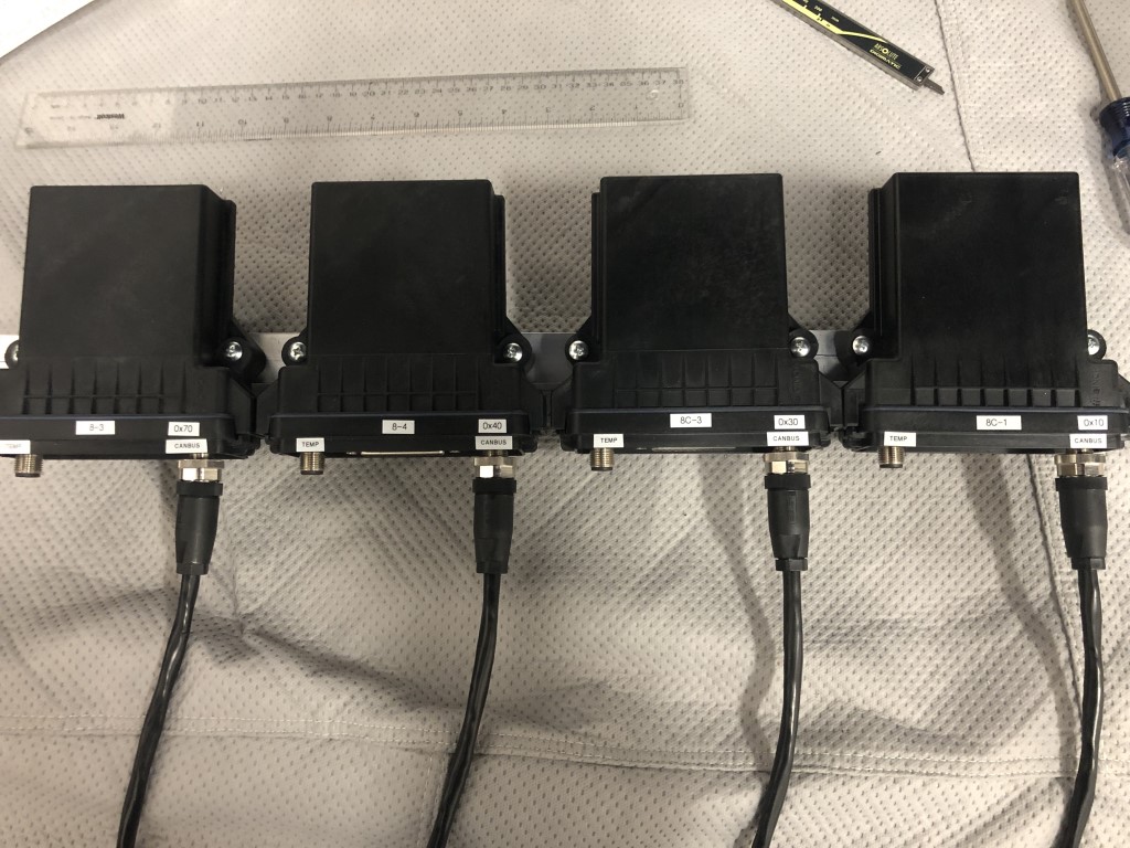
By mounting the BMS units inside the battery box negates the need to make the DB25 connectors any longer. The ones that are already connected to the batteries are used with a gender changer DB25 connector. Only the middle battery has to have a DB25 extension cable because that battery is wired in reverse order. I first tried to use the four 12mm wires shown above connected to each BMS in the battery box, but there is not enough room and it looked very cluttered. Plus I could not get all four wires though the hole in the side of the battery box. Using the 12mm tee connectors shown below have made the 12mm wiring more compact and only one wire has to come out to connect to all four BMS units. I need to add some cable management and strain relief to the one cable going though the side of the battery box.
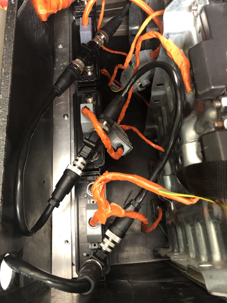
This initial setup is okay for testing. The battery sense wires (orange) will have to have some kind of wire management now that they are going to be connected all the time. I might also install the screws in the DB25 connectors once everything is tested and working correctly. The 12mm cables for the temperature measurement still have to be installed.
These are the12mm tee connectors that made a cleaner installation. Here is the link to the data sheet.

Update 5/3/2025:
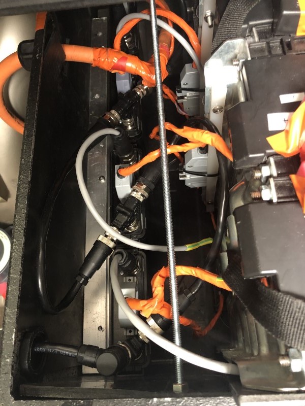
Installed wire management and all the temperature measurement cables. I used different 4-conductor cables for the temperature measurement. They were easier to connectorize with the 12mm connectors. I found I had to add a couple of threaded rods to hold the batteries tightly in the battery box. A while ago I had to cut the end of the box off when I added the fourth battery to the trunk box. I had a metal square tube as a strength member to hold the battery box together. I had to remove that tube where it was originally mounted. It was connected to the angle aluminum that the BMS units are attached to now. The threaded rod also makes it easy to adjust the compression on the box to hold the batteries so they don't move while driving.
- Details
BMS Readout PCA Redesign 4
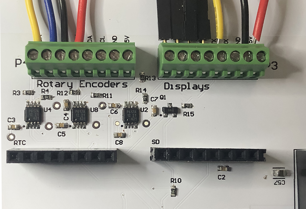
I received the new PCB and built up one assembly with the I2C driver ICs that were described in the Blog below, BMS Readout Redesign 3 (link). The PCA worked to read the RTC and SD card but failed to initialize the Rotary Encoders and the LCD did not show any text. After some checking I remembered that I had swapped the I2C lines in the PCB design to make the layout better with less crossing of data lines going to the screw terminals, but did not update the silkscreen text for each pin. Once I swapped the wires for the I2C data lines everything worked! The I2C line drivers did the job. The 7-segment display, that was being driven by the MOSFET logic level shifter also worked.
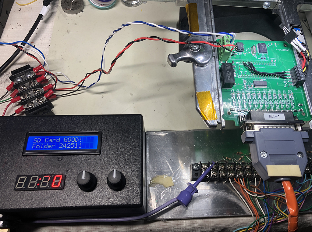
Below is an image of the New PCA, showing the I2C driver ICs (U2,U4,U8) and the MOSFET (Q1) logic level shifter circuit. I made the PCB a different color to tell the different versions apart.
I connected everything in the enclosure and ran the 9 BMS simulation test program. It worked perfectly. Now I can think about deploying the reader in the car.
Below is an image of the BMS simulation test bench setup. The BMS PCA on the right is connected to a barrier strip with a series of resistors. The circuit simulates ten battery cell voltages. It is connected to the reader via the CAN BUS wires (blue-white). I developed this test method over a year and a half ago in July 2023 to test the BMS PCA (link).
- Details
BMS Readout Redesign 3
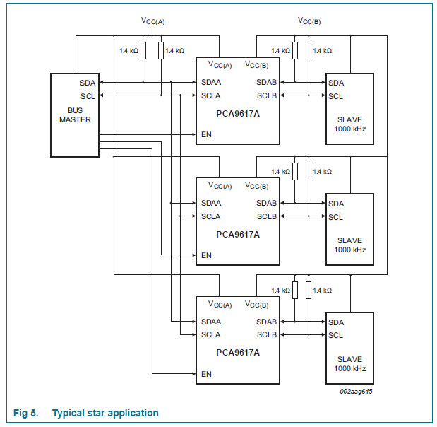
I thought that the Texas Instruments logic-level shifter integrated circuit was going to solve the problem with the different voltage logic levels in the BMS Reader Redesign 2 (see blog below). Initially it did work, the RTC and SD card worked without any issue. Those two components are mounted on the PCA, so they are connected to the logic-level shifter via traces on the PCA. When I first did the bench test to test the Arduino Nano 33 IOT and the logic-level shifter on the new PCA, I used only one Rotary Encoder with the LCD and the PCA was on the bench. That all worked without issue and I able to run the loop test program, simulating nine BMS units, which it passed. Once I put everything in the enclosure that is when I started having problems with I2C communication. When I connected the LCD and the two Rotary Encoders, using the screw terminals I found the Encoders would not initialize. If I disconnected the LCD the Encoders would connect. The Encoders and LCD are on the I2C bus. After doing some more research on the Texas Instruments device I found that it is very sensitive to the capacitance loading of the data lines. The RTC is a I2C device, but as I said it is connected to the logic-level shifter via traces. PCA traces have much smaller capacitance compared to free hanging wires. The 7-Segment display data lines also go through the logic-level shifter and are connected to the screw terminal via wires, but Serial is a much slower communication standard and hence it is less sensitive to the connection capacitance. The problem is with I2C communication - it is high speed so it is sensitive to the capacitance of the connection. So the multiple wire connections (two Encoders and a LCD) caused the issue. The real problem stems from the logic-level shifter. It was not designed to connect to many I2C slave devices, unless they are all PCA mounted and are connected via traces that have low capacitance. The capacitance issue has long ago been identified as a problem with I2C communication. Because it was initially developed for communication between devices mounted on a PCA and connected via traces (i.e. low capacitance). But now it used to connect many external devices, via wires. Devices have been developed to solve this problem. They are called I2C line drivers and can be connected in a pattern like the schematic below, to connect many external I2C devices to one master source. This particular line driver, the PCA9617A is made by NPX Semiconductors. The data sheet can be found here, which is the source of the figure below. In the figure, all the lines on the Bus Master side would be PCA traces and on the Slave side will be the screw terminals with the wire connections. The output of the line driver can drive much higher capacitance. Each wired connection will have its own I2C line driver. These devices can also function as a logic-level shifter so it solves two problems. As shown in the figure, the driver IC also has an enable connection. This can be used to control communication by enabling only the driver for one component communication. But in my Reader design all the I2C components are queried sequentially in the code. So there is no issue with communication collisions, which can happen if multiple devices try to communicate at the same time. The issue now is that a new PCA has to be designed and built and tested.
Update: After some design considerations that I realized from working on the new schematic and PCA layout, I decided to eliminate the logic-level shifter IC. Both the RTC and the SD card will work at 3.3V so I am going to change the schematic to use those components at 3.3V and communicate with them directly from the Nano 33 IOT. The I2C line drivers will be used for the other components that are connected by wires through the screw terminals. For the Serial communication to the 7-segment display I will use the MOSFET method for logic-level shifting, like this product from Sparkfun. I can incorporate one of those MOSFET circuits in my design: a single N-MOSFET transistor with two resistors is all the is needed for one channel.
Update2: The I2C line drivers were tested on the bench and found to function perfectly. Even with connecting two rotary encoders and the LCD to one PCA9617A output!
A new PCB was designed and ordered, one that incorporates the I2C line drivers and N-MOSFET logic-level shifter circuit. The new PCB will take about a week to be fabricated and shipped.
To see the latest in the BMS Reader redesigns click here.